Sony’s newly unveiled X-ray CMOS sensor promises record-breaking imaging speeds and low-noise performance, specifically engineered for inspection and measurement instrumentation. By merging high-accuracy energy measurements with photon-level data acquisition on a single chip, it aims to set a new benchmark in X-ray imaging technology.
Subscribe
Hardware Reviews
Sony Semiconductor Solutions to Release X-ray CMOS Sensor with Industry’s Fastest(*1) Imaging and Low-Noise Performance for Inspection and Measurement Instrumentation
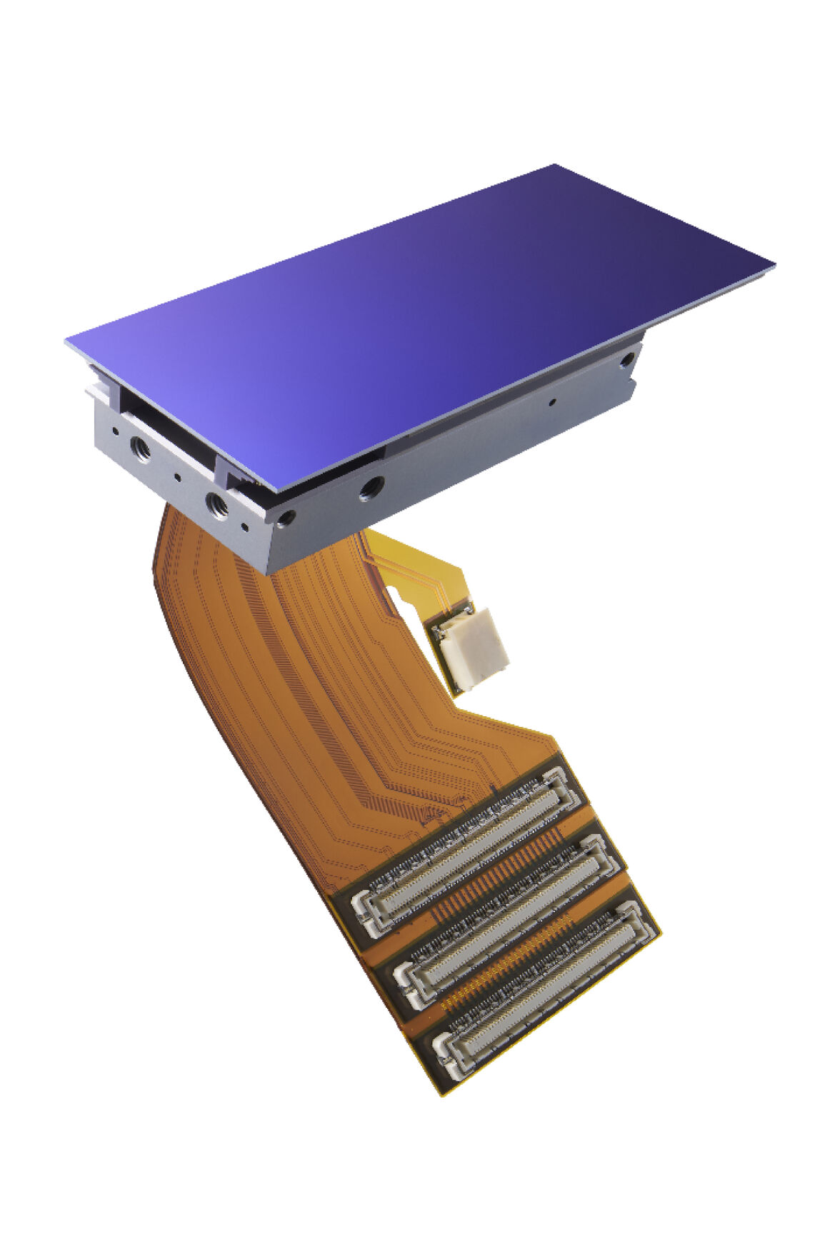
Photo by Yoursun.com
Key Takeaways:
- Sony’s latest release is an X-ray CMOS sensor boasting exceptional speed and low-noise performance
- The sensor is designed for inspection and measurement instrumentation
- Its single-chip architecture enables high-accuracy energy measurements
- Photon-level data acquisition is a central feature
- The product release date marks a significant milestone for industrial imaging
Overview
Sony Semiconductor Solutions has announced a new X-ray CMOS sensor that it touts as the industry’s fastest(*1) imaging solution, combined with low-noise performance. The company underscores the sensor’s utility in inspection and measurement instrumentation, promising enhanced clarity, speed, and precision for complex imaging tasks.
Advanced Technology and Design
One of the sensor’s most notable qualities is what Sony describes as “high-accuracy energy measurements and photon-level data acquisition on a single chip.” This advanced design aims to deliver exceptional clarity even in challenging imaging conditions, a critical requirement for fields that often rely on minuscule or delicate measurements. With photon-level data capture, the sensor can detect extremely low levels of X-ray signals, enhancing overall reliability and image resolution.
Inspection and Measurement Applications
The new sensor is squarely targeted toward professionals involved in inspection and measurement. By integrating speed and low-noise performance, Sony’s sensor could offer quicker processing times in environments where every millisecond matters. Whether it’s performing minute dimensional checks or analyzing material structures, the technology is expected to reduce errors and streamline workflows.
Conclusion
Scheduled for release under Sony Semiconductor Solutions, this X-ray CMOS sensor represents a leap forward in the ongoing push for greater precision and efficiency in industrial imaging. Its combination of speed, low-noise operation, and photon-level sensitivity stands to influence a range of vital applications within the inspection and measurement sector, marking an important development for researchers and engineers alike.